


HOME > Product Info > Reference Room
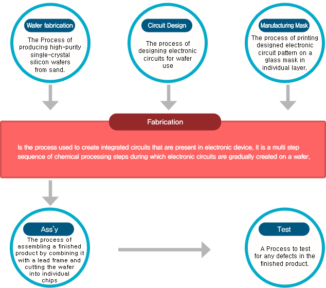
Refine semiconductor process
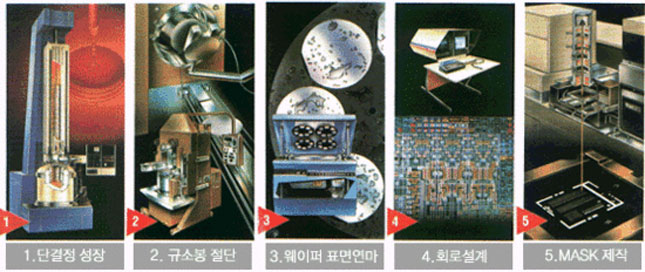
1) Polysilicon creation
Growth of a single crystal silicon rod is by melting high purity silicon and then cause it to solidify very slowly in contact with a single crystal “seed” (the term “growing” is used because it started from a seed)
2) Wafer slicing
Grown silicon rods cut into thin wafers for uniform thickness. Cutting is the word used to describe wafers depending on the silicon rod diameter 3”, 4”, 6” and 8” in order to improve productivity and the tendency for possible larger apertures.
3) Lapping & Polishing
Creating a polished surfaced like mirror by polishing one side of the wafer.
4) Circuit Design
Designing electronic circuits. Circuit patternis drawnon the wafer using a CAD System.
5) Pattern preparation
Designing a circuit pattern drawn on a glass mask with the use of an E-beam equipment.
Photomask is an opaque plate with holes or transparencies that allow light to shine through a defined pattern.It shields light and absorbs light corresponding to the light shield pattern.
(Similar to develop films.)
* Mask : Mask is used as a photo process by drawing a circuit pattern on the glass shape in each floor of the wafer stepper.
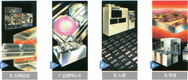
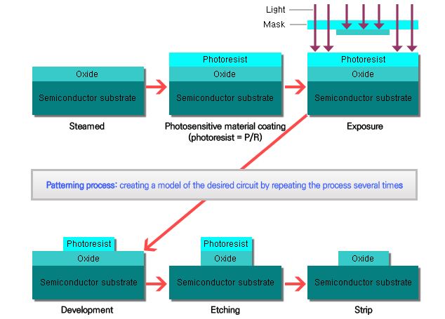
6) Oxidation layering
It refers to the process of forming gas silicone oxide (sio2) on the silicon wafer surface ( uniform thickness and in high temperature (800-1200 degree Celsius) by chemical reaction to oxygen and water vapor.
7) Photoresist coating
Is a light sensitive material used, to form a patterned coating on a surface. The M Aligner grill a picture taking device spreads evenly the coating on the wafer surface.
* Photoresist(P/R) : Circuits for Photo Resist developing
* Coater : Photo resist coating equipment.that evenly coats the photoresist on the wafer surface.
* Aligner : Sorter. The location on the wafer, and the mask repeatedly projected reduction is aligned to exactly match the fine circuit pattern.
8) Stepper Exposure
PR Film is formed on the wafer circuit pattern. It refers to the process of taking photos and the light that passes through the circuit pattern drawn on the mask.
(Semi Conductor Processing is one very important process.)
* Stepper : Camera for semiconductor manufacturing. Images is focus and reduced by a lens and projected onto the surface of a wafer that is coated with a photosensitive material called photoresist.
9) Develop
Photoresist is exposed to a pattern of intense light. The exposure to light causes a chemical change..Some photoresist becomes soluble in the developer when exposed and also the unexposed.
* Developer : The Developer has the capability to maintain the photo resist properties once exposed to light.
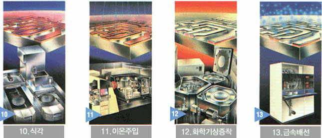
10) Etching
Process to selectively removed parts not needed. Chemical (wet) or reactive gas(dry) forms a circuit pattern leaving the remaining portion for its corrosiveness. Photo resist is then removed with a solution of sulfuric acid after the etching process.
The same process as Etching. Etchings production is the process of drawing a picture on top of a fire with a sharp awl by scorching the surface on the copper plate coated with paraffin, And with the use of that sharp awl, the paraffin is then peeled and corrosive chemical can be place. The picture is complete when chemicals and paraffin has been washed out. The pattern formation process is continuously repeated for each pattern layer semiconductor.
(Patterning process)
* Etcher : Equipment needed as part of a pattern formed on the wafer.
* Asher : Semiconductor processing equipment for dry removal of hardened photoresist by dry etching or implantation(Dry Strip)
* Stripper : Equipment that removes the photoresist remains after the etching process.
* Station : Station equipment used for wafer cleaning after every processing.
* Patterning process
11) Ion Implant
Makes the impurities in the circuit pattern associated with the acceleration in the form of tiny gas particles which is penetrated into the interior of the wafer by the characteristics of the electronic devices. Doped by the diffusion process to spread to the inside of the wafer by injection, impurity particles in a high temperature furnace is done.
* Implanter : Implanter is an ion implantation device. It consist of an ion source where ions are electrostatically accelerated to a high energy and a target chamber, where the ions impinge on a target which is the material to be implanted. High and Medium implants are used depending on the degree of acceleration.
* Spread : "spread", a substance that spread into any other material. It can be seen over the crystal clear water if the ink or ink spread is dropped into the water. The spread between solid-state semiconductor process spread liquid is made of high temperature environment of the rapid spread of processing necessary. It creates an environment of high temperature like a furnace. How you put the coil wound on the quartz tube furnace and wafer in a semiconductor line, is dependent on the blast furnaces and steel mills that use the horizontal or vertical type.
12) CVD
Particles formed by the chemical reaction of the gas sprayed in the form of water vapor (CVD) .A dielectric or conductive layer is formed on the surface of the wafer. CVD acts as a sort of a transient protective layer.
* CVD : CVD is a chemical process used to produce high purity high performance solid materials. The wafer is exposed to one or more volatile precursors which reacts on the substrate surface and once produced, volatile by products are removed by gas flow through the reaction chamber.
Deposition is divided into four kinds 1) atmospheric pressurechemical vapor deposition(AP CVD : Atmospheric Pressure CVD), 2) low-pressurechemical vapor deposition(LP CVD : Low Pressure CVD), 3) thermochemicalvapor deposition, 4) andplasma-enhanced chemicalvapor deposition(PE-CVD).
13) Metal Deposition
Gold, silver, aluminum wire are fabricated on some substrates using two layer resist method with reduced projection exposure and metal laminate deposition with electronic beam evaporation.
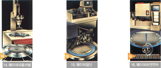
14) Electric Die Sorting
Chips are sorted and examined for defects.. If defective, it will be mark with a black ink.
15) Sawing
The process of separating the number of chips on the wafer by cutting the wafer using a diamond saw.
16) Die Attach
Process of attaching the chips to the pad or die cavity of the lead frame .Each die attaché process,use special tools and equipments to work properly.
* Lead Frame : Leg protruding like Centipede feet from the semiconductor and semiconductor electronics connected to the socket . Products that are sorted to be defective will be automatically excluded.
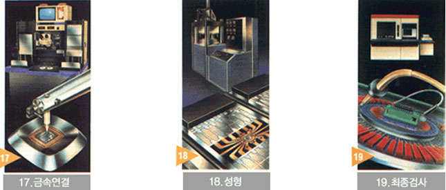
17) Wire Bonding
The process of providing elecrical connection between the lead frame chips and the external leads of the semiconductor using a very fine gold bonding wires.
18) Molding
The process of manufacturing by shaping raw material using a pattern. In this process we often see the shape of a foot black centifede.
19) Final Test
Final inspection and completion of the electrical characteristic of a semiconductor or computer is spilled in a high electrostatic force. If the product is working properly and can withstand high temperature and high and low humidity, then it will be ready to market.
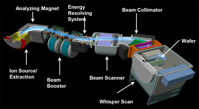
Implant Process
Definition - The process of injecting ions uniformily from a gas source so that the purity of the source can be very high.
The Role of the Implant Process
- - Adjust the electrical characteristics of semiconductor devices by aTransistor
- - Technology to inject impurities into the silicon substrate
Advantages and disadvantages of the Implant
● Advantages
- - Required amount of impurities may be injected
- - Low horizontal spread
- - Processing in low temperature
- - Precision, by controlling on how to maintain excellent reproduction
● Disadvantages
- - The most complex and expensive semiconductor equipment
- - Occurrence of damage during implantation
- - Damage may be inflicted by silicon lattice
Implant Terminology
- (1) Energy : Dopant control the depth upon entering the Wafer
- (2) Dose : the concentration of impurities
- (3) Dopant : Types of impurities
- (4) Beam Current : electrical representation of the amount of impurities to be injected per hour.
Component of the ion implantation equipment
- (1) Source : an ion source for producing a process gas and generating an electron beam to ionize the process gas within the Arc chamber
- (2) Beam line : extraction of ions from the source by injection, for focus and faster acceleration
- - Mass Analyzer : Mass Analyzer takes ionized masses by ION Beam electromagnet and separates them based on charge to mass ratios and outputs.
- - Acceleration : determines the depth of the Ion injected in the Ion Beam Wafer
- - Focusing : Beam prevent the spread
- - Scan : To spread the Ion Beam Wafer injection
Principles of ion implantation
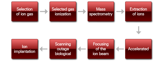
ION Implanter configuration