


HOME > Product Info > Reference Room
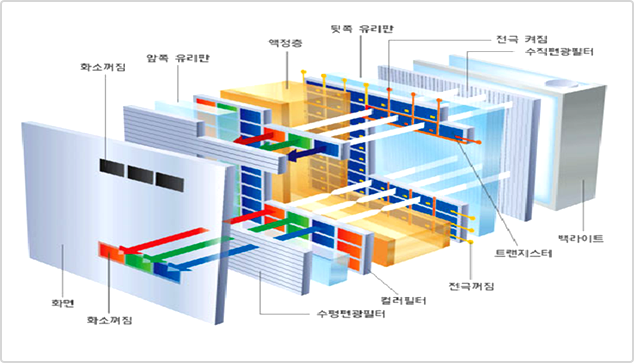
L.C.D?
LCD Is a Liquid-crystal display that uses light properties of liquid crystals. An electronically modulated optical device made up of any number of segments filled with biographical information and transformed into visual information.
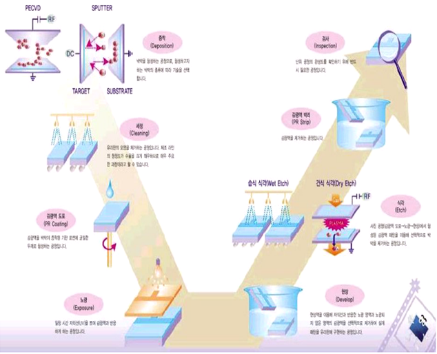
T.F.T(Thin Film Transistor) PROCESS schematic diagram
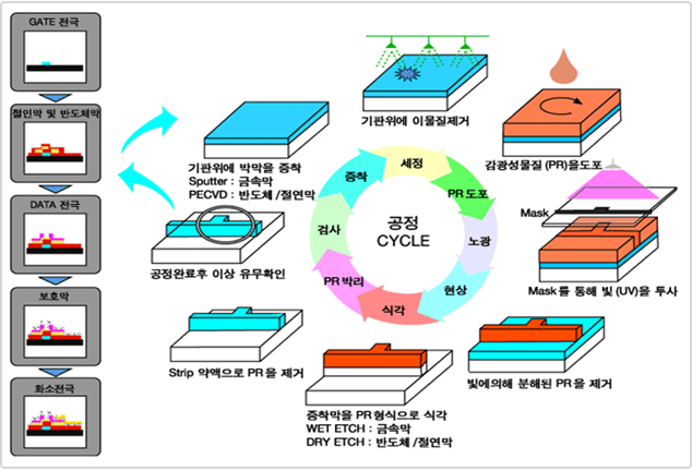
- According to the pattern forming process, each step in the process should be repeated one or more times, A repeated pattern formation process consists of processes such as thin film deposition -> exposure -> etching, -> as shown in the figure on the next, To check for cleanliness and to determine the results of the process before and after each cleaning. Metals and semiconductors, refers to the process of applying a thin insulating layer on the glass substrate thin film deposition process.
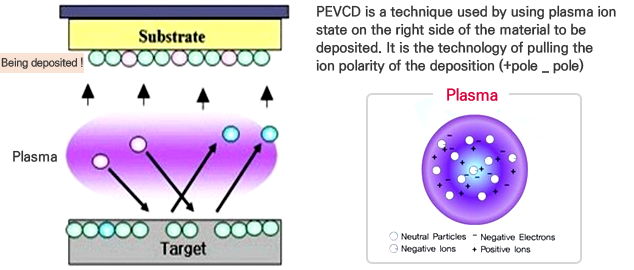
- sputtering method - Usage of Metal and ITO layer PECVD (plasma enhanced chemical vapor deposition) method. - Usage of silicon and insulating layer.
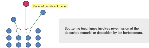
Sputtering & P.E.C.V.D deposition process - 1
A very clean glass substrate in a chamber is required in preparation for TFT Deposition.
- Clean Glass substrate.
- Deposited materials will be placed in the a glass substrate for TFT deposition.
- Deposition is a method of depositing material on a stable glass substrate.
- PECVD machine deposits thin films by sputtering, it involves eroding material from the source onto a substrate.
Sputtering & P.E.C.V.D deposition process - 2
After finishing the process, deposition should be clean. But, However clean it is, there still would be a problem and that is its disadvantage.
Schematic diagram PHOTO LITHOGRAPHY Process
Schematic diagram CELL PROCESS
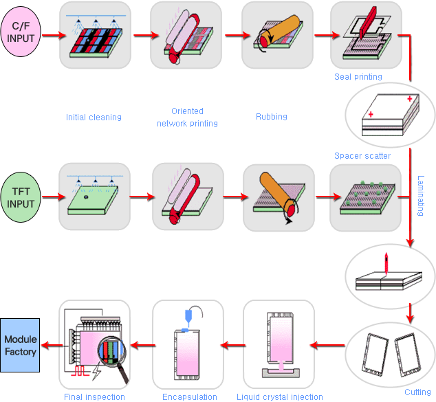
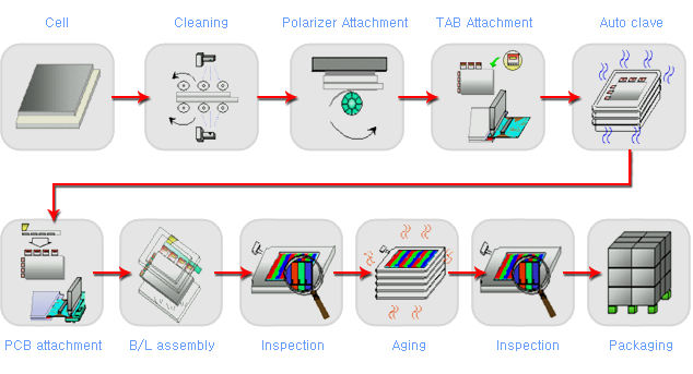
Schematic diagram MODULE PROCESS